Shape observation (2 positions)
$400/SampleProbe loss
$200/BatchMake up the difference
NegotiableSample
$50Testing Description
1.Surface morphology, thickness, and roughness testing of powder, solution, and bulk samples.
2. Surface morphology of biological/fiber samples
3.Phase diagram
4.PFM (piezoelectric force microscope), EFM (electrostatic force microscope), KPFM (surface potential), MFM (magnetic force microscope),
C-AFM/PeakForce TUNA (conductive force microscope), Young’s modulus/modulus distribution, force Special modes such as curve, submerged, and variable temperature.
For more test requirements, please feel free to contact us
Sample requirements
1. Sample status: it can be powder, block, film sample;
2. Powder samples: The particles are generally no more than 5 microns, 20mg is provided, and the liquid is no less than 1ml. If the size is too large, please con-sult the customer manager in advance;
3. For powderliquid samples, please note the sample preparation conditions, including dispersion, ultrasonic time and preparation concentration;
4. Film or block sample size requirements: length and width between 0. 53cm, thickness between 0.1-1cm, surface roughness no more than 5um, be sure to mark the test surface!
5. For testing piezoelectric and surface potential materials, samples need to be prepared on a conductive substrate, the size of which is larger than 0.5*0.5cm.
For other questions, please consult your account manager.
Examples
The form of the results of different models of instruments will be different. The following shows the results of Bruker Dimension ICON model AFM, for reference only.
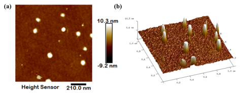
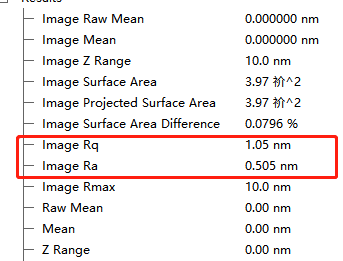
1. Surface morphology and surface roughness AFM can study the sample surface morphology, nanostructure, chain conformation, etc., and obtain information such as nanoparticle size, pore size, material surface roughness, material surface defects, etc. conditions change). The topography of the sample can also be displayed in a rich three-dimensional simulation, making the image more suitable for human intuitive vision. The figure below characterizes the 2D geometry, 3D height and roughness of the nanoparticles.
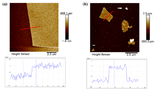
2. Precise positioning such as: nanosheet thickness/step height What is precise positioning? Just need to spend a little time to find this place. Measurement of high aspect ratio structures, such as trenches and steps, is often required during semiconductor processing to determine the depth and width of the etch. These can only be measured by cutting the sample along the cross section under SEM, and AFM can measure it non-destructively. The resolution of AFM in the vertical direction is about 0.1 nm, so it can be well used to characterize the thickness of nanosheets. The figure below characterizes the step height and nanosheet thickness map.
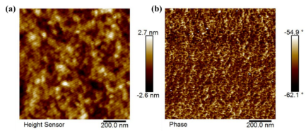
3. Phase diagram As an important extension of the tapping mode, the phase mode is determined by detecting the difference between the phase angle of the signal source driving the vibration of the micro-cantilever probe and the phase angle of the actual vibration of the micro-cantilever probe (ie, the phase shift of the two). change to image. There are many factors that cause this phase shift, such as sample composition, hardness, viscoelastic properties, modulus, etc. To put it simply, if the contrast between the two materials is relatively small in terms of AFM morphology, but you really want to explain what kind of film this is on, you can use the two-dimensional topography map + phase map to Description (provided that the physical properties of the two materials are relatively different, and the phase diagram has obvious contrast signals).
The test raw files of Bruker AFM instruments in .spm format can be opened with the Bruker offline software Nanoscope analysis software.
FAQs

Resources
+65 94778355
Service Hotline: +65 94778355 Copyright © 2022 ANR Technologies Pte Ltd