Morphology
S$133++EDS-Point Scanning
S$39 per sampleEDS-Line Scanning
S$78 per sampleEDS-Mapping
S$117 per sampleDiffraction
S$39 per sampleStem (haadf)
S$117 per sampleTesting Description
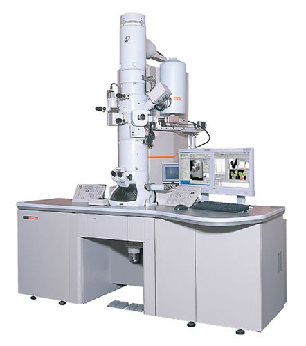
Transmission Electron Microscopy (TEM) plays an unobtainable and important role in the fields of materials science, life science, chemistry, physics, metal materials, etc. It can obtain microscopic materials such as metals, minerals, semiconductors, polymers, ceramics, composite materials, and nano Microstructure, high-resolution crystal structure, microstructure, etc. are very important for studying the microstructure of materials and exploring the mechanism of materials. Through TEM morphology analysis, the following information can be obtained:
1. Obtain the microscopic morphology, porosity, sample particle size, etc. of nanomaterials, metal materials, and ceramic materials;
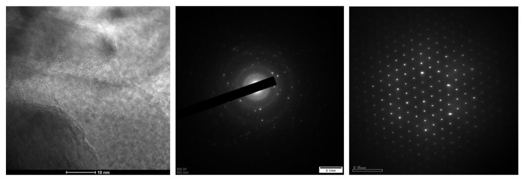
2. Obtain high-resolution data of materials, lattice fringes, and crystallographic parameters;
3. Obtain material diffraction pattern and judge material crystallographic parameters;
4. Obtain the material EDS signal, characterize the material element distribution, semi-quantitatively analyze the material element content, etc., and can perform surface scan, point scan, line scan, etc.;
5. With STEM mode, it can collect four kinds of images from different angles of electronic signals including bright field (BF), annular bright field (ABF), annular dark field (ADF) and large angle annular dark field (HAADF);
Sample requirements
1. Sample Status
Both powder and liquid samples are acceptable. Films and blocks cannot be tested directly. Please explain and confirm in advance if ion thinning, double spray, FIB, and slice sample preparation are required.
2. Sample composition requirements
This instruction is only for material testing samples, biological samples are completely different from materials. Generally, the test samples have the following requirements:
Safety: non-toxic, non-radioactive;
Whether it contains organic objects: Organic objects is unstable under high pressure, and is easily broken up during the shooting process. When the sample is broken up, it will contaminate the instrument. If you need to shoot, please confirm with our staff. Samples with organic objects cannot be photographed for mapping, please do not select this option when making an appointment; Magnetic: Magnetic particles are easily adsorbed to the pole pieces. In principle, electron microscopes (SEM and TEM) do not capture magnetic samples. For magnetic sample, please confirm with our staff first.
Magnetic samples: Magnetic samples containing iron, cobalt, nickel, manganese, etc. are all magnetic samples. Note that magnetism is divided into hard magnetism and soft magnetism. Some materials do not exhibit magnetism to the outside world, but are easily magnetized after applying a magnetic field, and the magnetic enhancement after heating also needs to be defined as a magnetic sample.
Strong magnetism: A sample that can be picked up by magnets. Weak magnetism: A sample that cannot be attracted by magnets but is magnetic as defined above.
3. Selection of copper mesh
Generally, copper mesh is used for ordinary topography samples, and ultra-thin carbon film or microgrid is used for high resolution; If the sample is flake, or larger than tens of nanometers, micro-grid can be used to see high resolution (micro-grid has no substrate, and the middle is hollow);
If the sample is smaller than 10nm, it is not recommended to use a microgrid, because the sample will not be fished;
For quantum dots or small particles of 10nm, only ultra-thin carbon film can be used, and the relative contrast is not very good; for the mapping, C element is used, and microgrid is used, and the sheet sample is required to be just in the middle of the copper mesh hole. The carbon film exists because there is also a carbon film on the microgrid skeleton;
Copper mesh, ultra-thin carbon film, and microgrid all contain Cu element. If the sample is just on the skeleton, it will be scanned to make Cu element. Generally, molybdenum mesh is used instead, but the high-resolution effect of ordinary molybdenum mesh is not good.
Examples
FAQs

Resources
+65 94778355
Service Hotline: +65 94778355 Copyright © 2022 ANR Technologies Pte Ltd